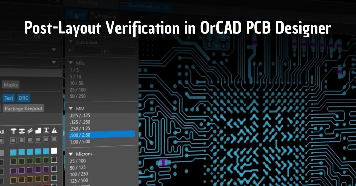
In the realm of PCB design, the journey from concept to production is fraught with challenges that require meticulous attention to detail. One of the most critical stages in this journey is post-layout verification. This process ensures that the design meets all specified requirements and is free from errors before it goes into production. OrCAD PCB Designer, a powerful tool in the PCB design industry, provides robust post-layout verification features that help designers streamline this crucial phase. This article delves into the significance of post-layout verification in OrCAD PCB Designer and the steps involved in ensuring a flawless PCB design.
Understanding Post-Layout Verification
Post-layout verification is the process of checking the final PCB layout against design rules, electrical constraints, and manufacturing requirements. This step is essential to catch any potential issues that could compromise the functionality, performance, or manufacturability of the PCB. Errors caught at this stage can prevent costly rework and delays in production, ensuring that the final product meets quality standards.
Key Features of OrCAD PCB Designer for Post-Layout Verification
OrCAD PCB Designer offers a comprehensive suite of tools for post-layout verification, each designed to address different aspects of the verification process:
- Design Rule Checking (DRC) Design Rule Checking is a fundamental feature that ensures the PCB layout adheres to predefined design rules. These rules cover various aspects such as trace widths, spacing between traces, component placement, and via sizes. OrCAD PCB Designer’s DRC tool runs automated checks across the entire layout, identifying any violations and highlighting them for the designer to address.
- Electrical Rule Checking (ERC) Electrical Rule Checking goes beyond physical layout rules to ensure electrical integrity. This tool checks for issues such as unconnected nets, short circuits, and incorrect component orientations. ERC in OrCAD PCB Designer helps prevent electrical faults that could lead to malfunctioning circuits.
- Signal Integrity Analysis Signal integrity is crucial in high-speed PCB designs where issues such as crosstalk, reflection, and signal attenuation can occur. OrCAD PCB Designer includes tools for signal integrity analysis, allowing designers to simulate and analyze the behavior of signals on the PCB. This analysis helps identify and mitigate potential issues that could affect the performance of the final product.
- Power Integrity Analysis Ensuring a stable power distribution network (PDN) is vital for the reliable operation of a PCB. OrCAD PCB Designer’s power integrity analysis tools enable designers to simulate and verify the power delivery to all components, checking for issues such as voltage drops and noise.
- Manufacturability Checks OrCAD PCB Designer includes design for manufacturability (DFM) checks that ensure the PCB can be manufactured without issues. These checks verify that the layout meets the requirements of the fabrication and assembly processes, such as minimum feature sizes and proper solder mask coverage. By integrating PCB layout services, designers can further optimize the layout for manufacturability, ensuring a seamless transition from design to production while minimizing potential errors and production costs.
Steps in Post-Layout Verification
The post-layout verification process in OrCAD PCB Designer typically involves the following steps:
- Run Design Rule Checks (DRC) Start by running the DRC tool to identify any design rule violations. Address each violation by modifying the layout as necessary.
- Perform Electrical Rule Checks (ERC) Next, run the ERC tool to ensure electrical integrity. Resolve any issues such as unconnected nets or short circuits that the tool identifies.
- Conduct Signal Integrity Analysis Use the signal integrity analysis tools to simulate the behavior of high-speed signals on the PCB. Make any necessary adjustments to mitigate signal integrity issues.
- Verify Power Integrity Run power integrity analysis to check for stable power delivery. Address any issues such as voltage drops or excessive noise.
- Execute Manufacturability Checks Finally, run DFM checks to ensure the layout meets manufacturing requirements. Make adjustments as needed to comply with fabrication and assembly constraints.
Conclusion
Post-layout verification is an essential step in the PCB design process, ensuring that the final layout is error-free and meets all design and manufacturing requirements. OrCAD PCB Designer provides a comprehensive set of tools for this purpose, including DRC, ERC, signal and power integrity analysis, and manufacturability checks. By leveraging these tools and integrating PCB design services, designers can effectively manage complex design challenges and optimize layouts for manufacturability. This approach not only prevents costly rework but also ensures a smooth transition to production, crucial for maintaining competitiveness in industries where quality and time-to-market are paramount. The post-layout verification capabilities of OrCAD PCB Designer, combined with expert PCB design services, are instrumental in delivering reliable and high-performance PCB designs that meet the demands of today’s fast-paced technological landscape.


